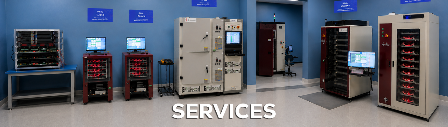
Semiconductor Test & Characterization
Full electrical characterization and functional testing of advanced semiconductor devices across temperature, voltage, and frequency conditions required for aerospace and defense qualification.
- DC parametric and functional test coverage
- Temperature characterization from cryogenic to high-temp
- Custom test program development for complex ASICs
 01
01
 02
02
High-Power Device Testing
Specialized test infrastructure for high-power semiconductor devices including GaN, SiC, and high-voltage transistors used in power conversion and RF amplification applications.
- High-current and high-voltage device characterization
- Thermal resistance and power dissipation analysis
- Safe operating area (SOA) evaluation
RF and Millimeter-Wave Validation
Comprehensive RF characterization and millimeter-wave device validation supporting radar, electronic warfare, and satellite communications semiconductor technologies.
- S-parameter and noise figure characterization
- mmWave testing up to 110 GHz
- Load-pull power and linearity measurement
 03
03
 04
04
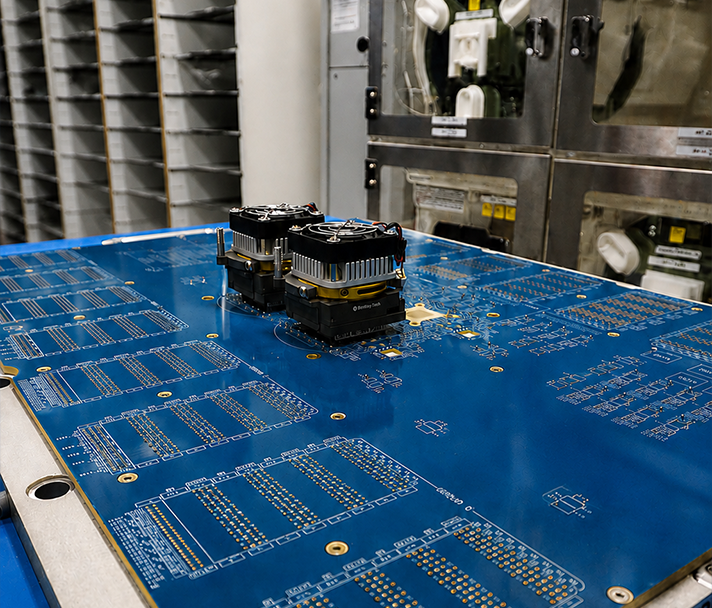
Load Board & Test Hardware Development
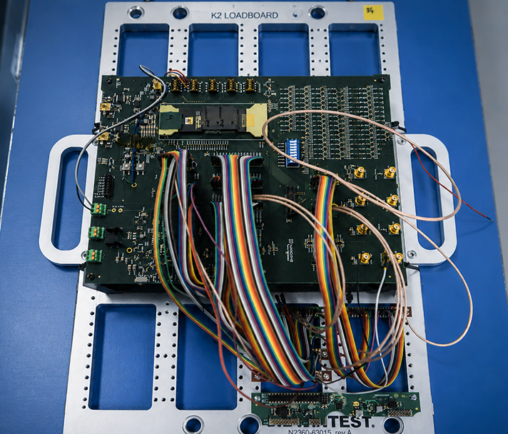
Custom load board design and test hardware development enabling precise electrical access to complex semiconductor packages used in aerospace and defense applications.
- Custom PCB design for ATE platforms
- High-frequency signal integrity optimization
- Thermal and mechanical interface engineering
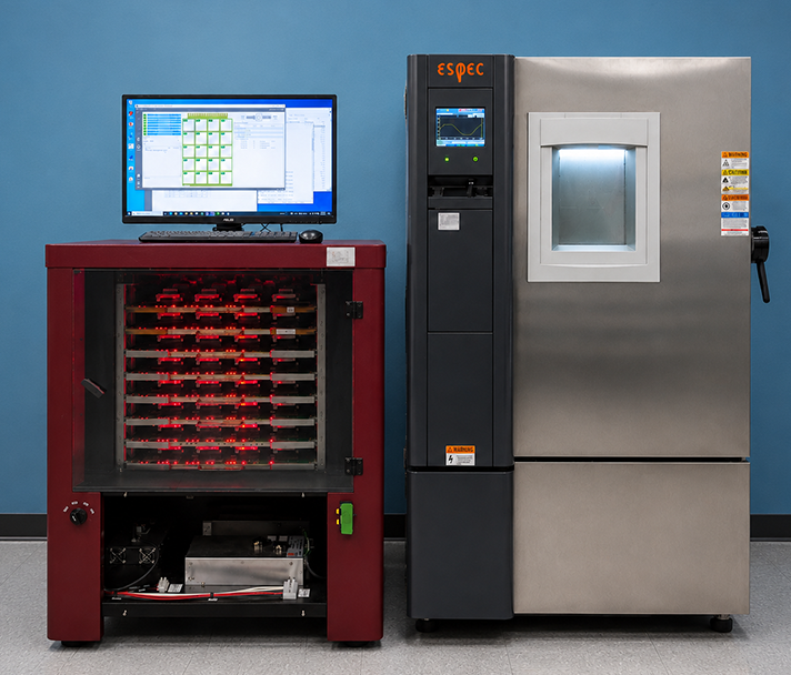
Reliability Screening & Burn-In
Structured reliability screening and burn-in programs designed to identify infant mortality failures and validate long-term device performance in mission environments.
- HTOL, HTSL, and temperature cycling programs
- Pre and post stress electrical testing
- Failure analysis and data reporting
 05
05
 06
06
Radiation Validation
Radiation effects evaluation including total ionizing dose (TID) and single event effects (SEE) testing to qualify semiconductor devices for space and high-radiation environments.
- Total Ionizing Dose (TID) evaluation
- Single Event Effects (SEE) characterization
- Radiation hardness assurance (RHA) support
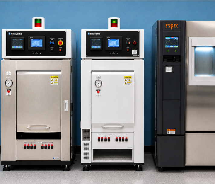
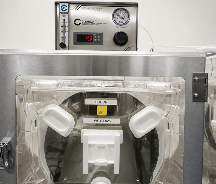
Environmental Testing
Environmental stress testing to validate semiconductor device performance under the thermal, mechanical, and atmospheric conditions encountered in aerospace and defense deployment.
- Thermal shock and temperature cycling
- Vibration, shock, and mechanical stress testing
- Humidity and altitude exposure programs
 07
07
 08
08
Logistics & Program Lifecycle Support
End-to-end program logistics and lifecycle management supporting semiconductor qualification from initial engineering evaluation through production and sustained program support.
- Program planning and qualification roadmap development
- Inventory management and device traceability
- Long-term program documentation and reporting
Electrical Test & Characterization
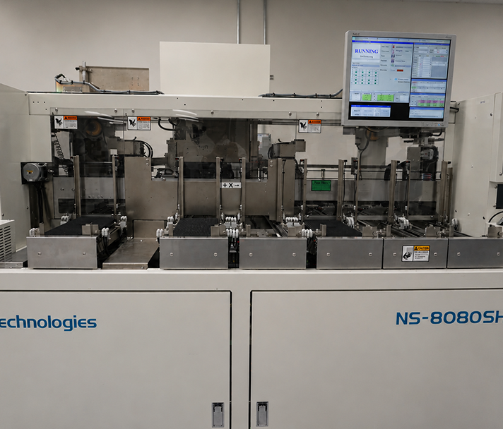
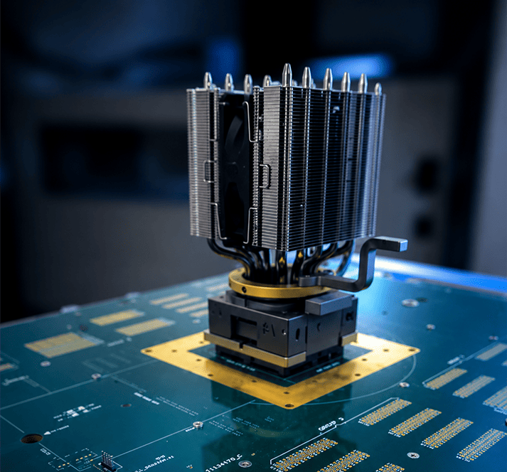
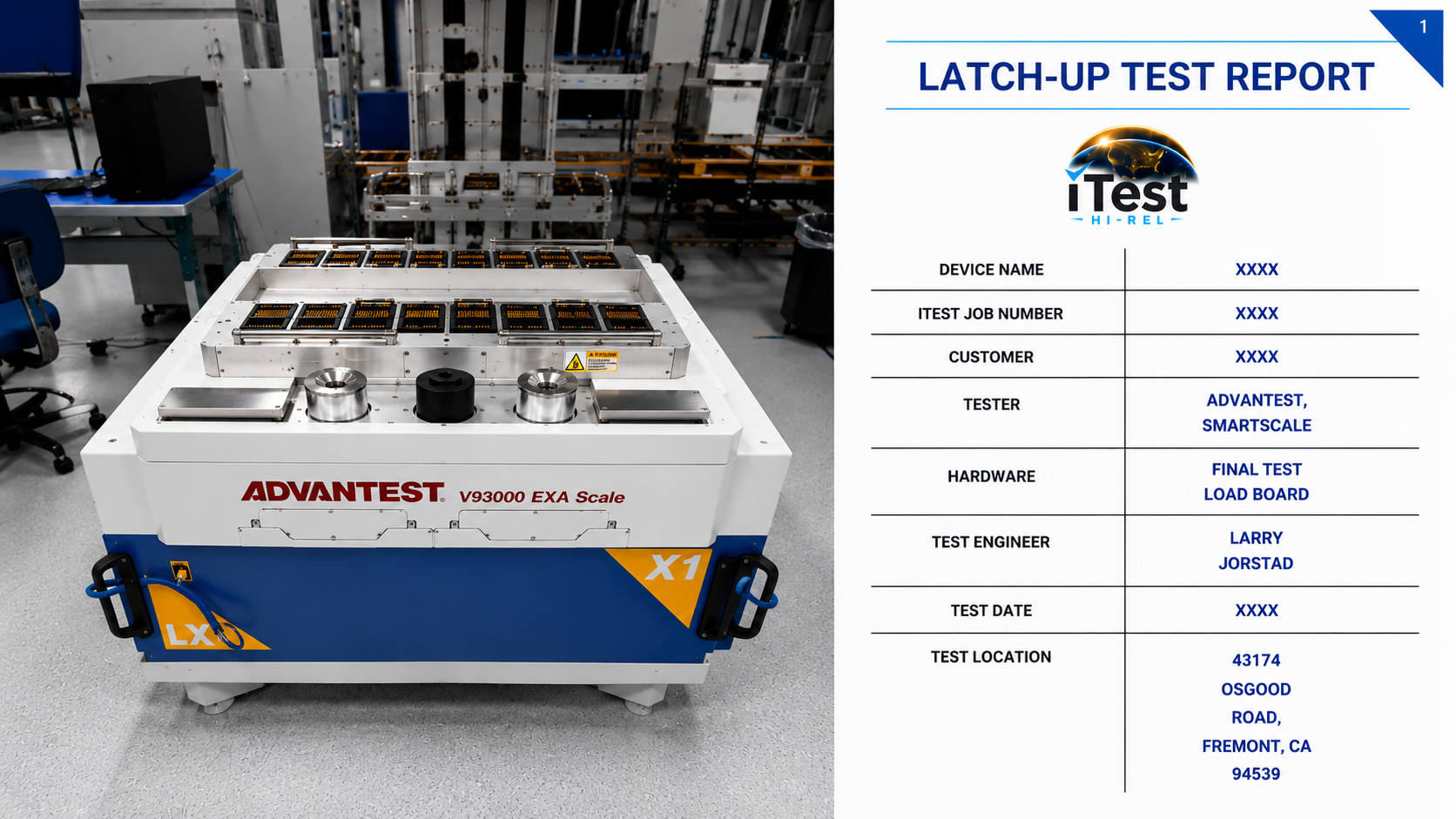
Advanced semiconductor characterization for high-performance devices—from ultra-high pin count and high-speed interfaces through RF and millimeter-wave coverage, high-power evaluation, and wafer sort / probe.
- Ultra-high pin count testing and exascale-class throughput
- High-speed digital interfaces and leading-edge instrumentation
- RF and millimeter-wave characterization; high-power device testing
- Wafer sort and probe; three-temperature wafer sort
- Automation, high throughput, and clean hardware environments
 09
09
 10
10
Mission Qualification & Reliability Services
Structured qualification and reliability programs for mission-critical semiconductors, combining environmental stress, burn-in, and electrical stress methods with precision ESD and latch-up coverage.
- Latch-up testing with ATE-based diagnostics
- ESD (HBM / CDM); robotic CDM with precision alignment and die-level capability
- HBM with dedicated boards and controlled parasitics
- HAST, burn-in, and environmental testing
Hardware & Interface Engineering
Dedicated hardware design and signal integrity engineering for complex ATE and mission interfaces—RF and high-speed connectivity, power and thermal engineering, and intelligent hardware systems.
- Dedicated hardware design and stack-up development
- Signal integrity engineering and RF & interface capability
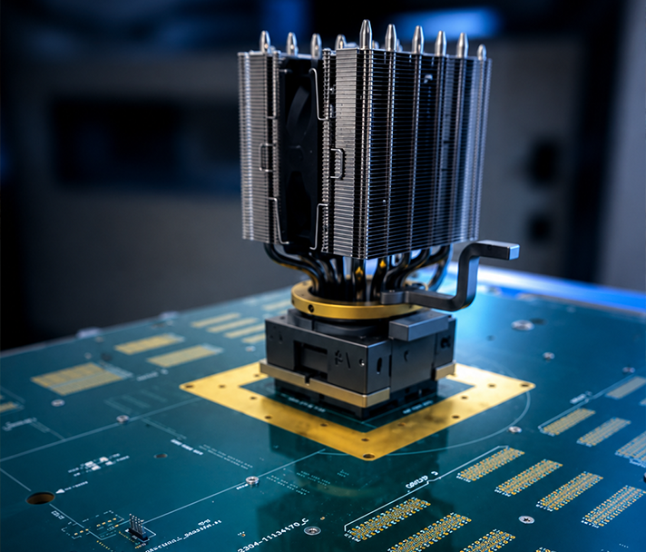
- Power and thermal engineering for demanding test conditions
- Advanced stack-up design and intelligent hardware systems
 11
11
 12
12
HTOL & Advanced Burn-In
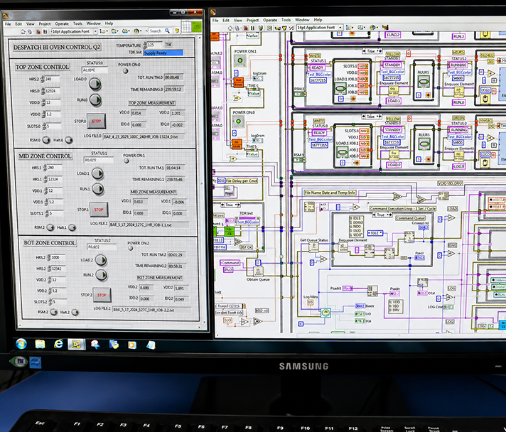
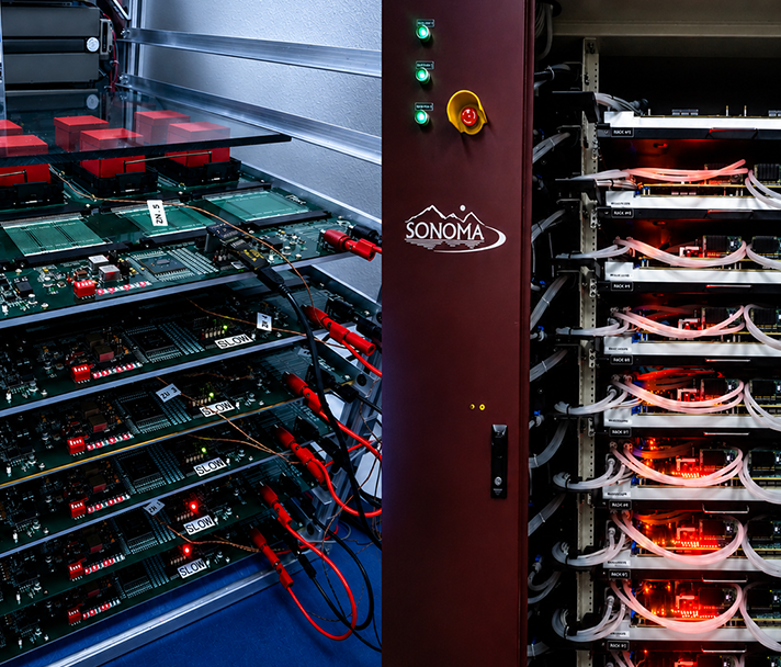
Burn-in treated as a reliability intelligence process—combining high-speed and high-power stress with thermal control, real-time monitoring, and diagnostics to surface early failures before deployment.
- High-speed and high-power burn-in with thermal control
- Real-time monitoring and early failure detection
- Thermal mapping and device-level diagnostics